Wakamiya Lab Research Projects
1. Chemistry of new 𝜋-conjugated systems
2. Creation of a functional 𝜋-electron system utilizing the characteristics of elements
3. Printable electronics: Development of next-generation solar cells
Molecules with 𝜋-electron systems have unique electronic, optical and magnetic properties. Various structures have been synthesized, such as cyclic hydrocarbons, annulenes, heterocyclic compounds, together with their cationic species and anionic species. Their exceptional electronic and optical properties make these useful materials for organic electronics, including organic transistors (OFETs), organic EL (OLEDs), and organic solar cells (OPV, DSSC, perovskite solar cells). Molecular electronics is multidisciplinary field, bringing together expertise in electronics, applied physics, as well as chemistry. At its foundation is the 𝜋-electron compound, however. The discovery of just one new molecule that exhibits truly superior performance can revolutionize the field. Our research approach is to apply feedback from the required functionality to synthesize materials based on a unique molecular design.
Model compounds are synthesized with unique molecular structures and elemental compositions. After the structure of 𝜋-electron compound and its physical properties are obtained, the performance of organic electronic devices such as solar cells using the synthesized material can be evaluated. With molecular design, synthesis, basic characterization, and device fabrication combined in a single research group, it is possible not only to measure the electronic and optical physical properties of the material, but also optimize the device fabrication process, examine the device stability, etc. By looking at the "needs" of the application, unsolved issues, unfinished technology, and unexplored research issues in modern chemistry and basic science will become clear. In our laboratory, Needs Inspired Fundamental Science is the core of our research policy.
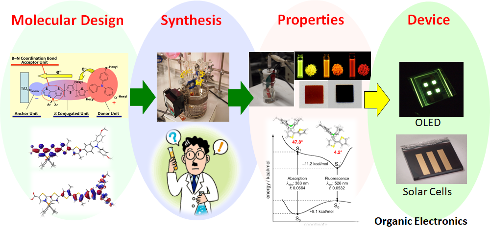
For example, in organic electronic devices the functional properties often depend on how the molecules line up or aggregate in solid state. In other words, on the details of the molecular assembly. We develop model compounds which establish a built-in control method for the molecular orientation and alignment in the solid state. Focusing on the thin films of these compounds, and using various spectroscopy methods, the correlation between the structure of the molecular assembly and the photo-electronic physical properties is clarified. Through this research cycle, we establish the basic science for creating high value-added organic semiconductors.
1. Chemistry of new 𝜋-conjugated systems
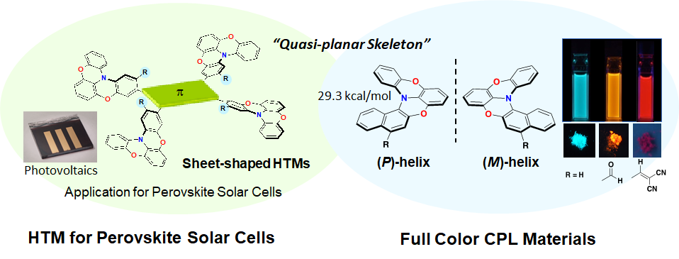
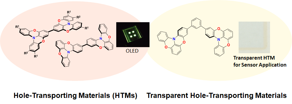
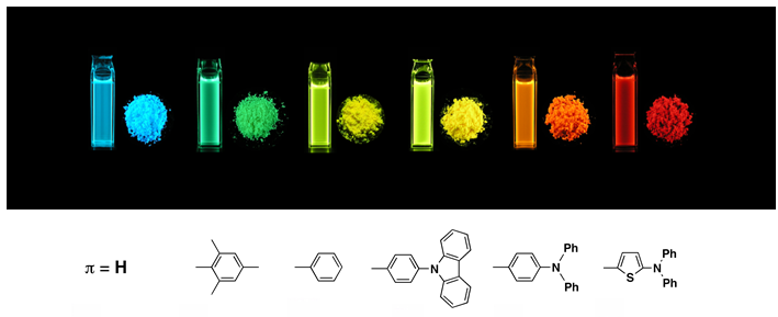
So how do you design molecules? The answers are found in the field of structural organic chemistry. A molecule is made to express a desired function by a unique design that assembles an 𝜋-electron containing element and extends this motif into a 𝜋-conjugated framework system through bonding. Such structural design can be said to be "molecular architecture". From the standpoint of experimental chemistry, the molecule must not end up as an abstract theory. It is important to always think about how to actually synthesize it. In addition to in-depth knowledge of electronic properties based on orbital interactions, "creative ideas" are vital. As an example from our own work, we designed a "quasi-planar framework" by bridging the three benzene rings of the triphenylamine framework with two oxygens. By twisting the framework a little, we could realize a one-dimensional stacked structure. These molecules function as organic hole transporting materials in organic electroluminescent diodes and perovskite solar cells. In addition, by changing the linkage mode of this skeleton, it is possible to develop a material having both high transparency and good charge transport properties.
2. Creation of a functional 𝜋-electron system utilizing the characteristics of elements
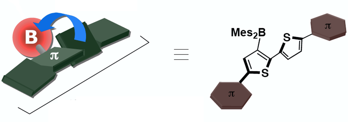
Atoms of various elements are combined to form a molecule, and by assembling them, they become substances and express functions. Knowing the properties of these elements and creating new functional substances is the essence of chemistry. One of our favorite elements is boron. Group 13 element boron has some unique structural and electronic properties: it has a three-dimensional planar structure, an empty p orbital, is a Lewis acid, and exhibits high 𝜋-electron acceptability in the photo-excited state. We propose a unique molecular design concept from the viewpoint of connecting these characteristics to the functional expression of organic materials.
3. Printable electronics: Development of next-generation solar cells
Nowadays, daily life is made convenient and comfortable by an abundance of electronics. Most microelectronics, as well as solar cells and LEDs, are based on inorganic semiconductors such as silicon. By replacing these with organic materials, features such as light weight, small size, and flexibility can be realized. The use of organic materials also makes it possible to fabricate devices inexpensively and rapidly by the use of solution processes i.e. printing techniques.
When comparing conventional inorganic materials and organic materials, however, we notice that from the viewpoint of molecular design there are many significant challenges. For example, inorganic materials have a network of three-dimensional bonds in the solid state and show excellent isotropic charge transport properties. In contrast, the charge transport in molecular materials relies largely on hopping processes between molecules and these depend on the overlap between 𝜋-orbitals of adjacent molecules in the solid state. In other words, the design of an organic semiconductor material with excellent charge transport properties requires, in addition to the control of the molecular electronic structure, careful control of the molecular assembly and packing structure in the solid state.
We tackle the issue of molecular alignment and orientation through unique molecular design and the synthesis of target compounds, together with the preparation and evaluation of thin films and devices.
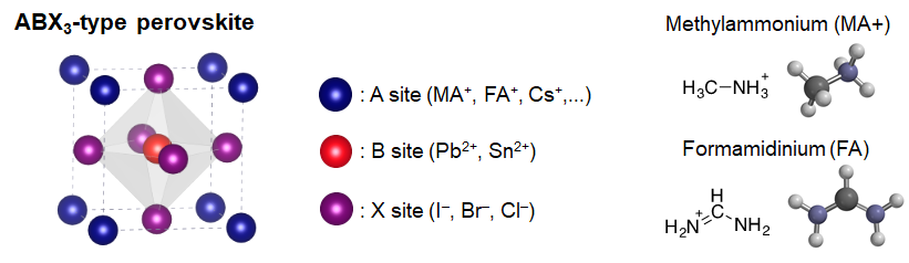
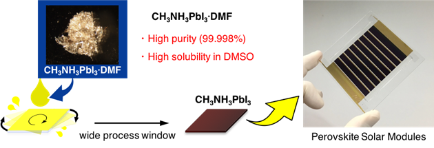
In recent years, research and development of solar cells and light emitting devices using ABX3 type perovskite semiconductor materials have attracted attention. We have already started this research, and are helping researchers improve the performance of photoelectric conversion devices such as solar cells and light emitting devices though the development of new starting materials and optimized fabrication methods. Although the ABX3 type perovskite is an inorganic material, it has many common points with organic semiconductor materials including solution-phase, low temperature processing. Previous research has shown that the purification of the starting materials is extremely important for efficient device performance. Thin film manufacturing methods based on the crystal growth mechanism from solution are is another important topic which we are involved in. We also examine the possibility of further enhancement of the device by combining the perovskite layers with tailor-made organic semiconductor materials. Based on these achievements, we have already achieved more than 20% photoelectric conversion efficiency, the first laboratory in Japan to do so. In 2018, we established "Enecoat Technologies Co., Ltd." as a venture company from Kyoto University, and we are also developing activities for implementation of these devices in society.
Home Projects Publications Contact Equipment Gallery Access Links Japanese